Sunday, December 4, 2011

Rescuing an ArduinoBT board

A few days ago I help a friend recover his ArduinoBT board. He had somehow managed to mess up the Bluetooth bootloader on the Arduino, and with wireless comms being the only way to program the board, he was stuck. I used my DIY BP BusPirate along with the STK500 firmware found on DangerousPrototype’s website to reflash the ATmega328 on the board. The process was reasonably straightforward as you shall see.

I used ds30Loader to update my BP’s firmware to the STK500v2 firmware. Doing this allows the BP to be used with AVRdude (download WinAVR for the most recent version of AVRdude).

imagesHeader connections: VTG to 5v, /Res to CS on the BP

I connected appropriate pins on the BP to the 6-pin programming header on the board as shown above. I then fired up AVRdude from the command line and burnt the appropriate firmware (found in “\arduino-0023\hardware\arduino\bootloaders”).

The standard firmware used by the ‘328 on the ArduinoBT initializes the Bluetooth module (a Bluegiga WT11). My friend had somehow managed to damage the firmware, and hence the WT11 was not being initialized at all.

I’m not too keen on using wireless to burn code onto microcontrollers. Its all fine and dandy, but when you’re prototyping, wireless is almost always the bad guy! So I decided that the best way for my friend to get new application code onto the board would be using a wired USB-to-serial converter, in this case, an MCP2200. I’m digressing, but the MCP2200 has custom open source firmware discussed here. Anyway, the bootloader that I finally burnt onto the BT board was actually the same one used on the Duemilanove board (“ATmegaBOOT_168_atmega328.hex”). This would hopefully allow me to dump code onto the ‘328 using a simple, no-fuss USB-TTLuart.

After burning the Duemilanove bootloader with the BP, I compiled the LED blink code with the Arduino IDE and tried dumping it onto the ‘328 with the USB-UART.  And as usual, things in electronics are not all hunky-dory: the WT11’s UART is connected to the ‘328’s UART; I was trying to connect a second UART to the ‘328. Can you see the problem here? Two trains on the same track? The WT11’s Tx was interfering with the MCP2200’s Tx. The only was to solve this was to perform a little open heart surgery on the board.

DSC02064 DSC02066
The ArduinoBT board with the TX line from the WT11 cut

Tracing the WT11’s Tx line on the board (found from the datasheet), I made a small cut in the trace using an exacto knife. I then scraped away solder mask on the trace and soldered a 3.3kohm 0603 resistor inline. This would allow the WT11 to send data to the ‘328, but would allow an external UART to be connected too. The external UART takes precedence, since it is directly connected to the ‘328 without a resistor.

DSC02067 DSC02069
Left:Too much flux never hurt anybody Right:after a quick iso-proply cleaning

The ‘new’ board is working fine, and the bootloader, if really required, can be reverted to the original.

Sunday, July 10, 2011

Reflow Soldering

I’ve been working with SMDs for quite some time now. Upto now I’ve been using a magnifying glass, a point tip, fine solder, and copious amounts of flux, but when you’ve got a bunch of chips with tiny little pins (or maybe even NO pins!) reflow soldering is the way to go.

Very tiny balls of solder suspended in flux form a sort of paste. This solder paste is applied to the pads over which the chip is placed. When heat is applied the solder balls melt, and helped by the flux the solder wets the pads/leads. On cooling, the solder forms a (usually) good joint.

Wanting to do a bit of reflow myself, I bought myself some solder paste (known as ‘PPD’ in Lajpat Rai Market). The paste seemed a bit dry, and in hindsight I should have added some more flux to it. But I’m getting ahead of myself. Let me tell you a bit about how I got my SMD soldered.

Normally, a stencil is used to apply the solder paste. Stencils cost a bomb to make, and spending so much just to solder a few boards is not worth it. I used Sparkfun’s tutorial as a reference, and also had a look at Fly Electric and Bill Shaw’s attempts.


The chips with flux and paste – I didn’t really care much about neatness. The surface tension of the solder ‘fixes’ itself.

I used one of my PIC’882 dev boards with an MCP2200 20pin SOIC, and an SOT23 LM1117. The solder paste came in a small plastic container. I used a flathead screwdriver to apply the paste. I fluxed the pins of the chips, and then used a pair of tweezers to place the chips on the board.

 
Left: The aluminium foil on the toaster tray ensures I don’t die of lead poisoning when I toast bread later.
Right: my new multimeter has got a cool thermocouple temperature sensor

I had a regular toaster that I placed the board in. To measure temperature I used my multimeter with a thermocouple. I wasn’t to particular about time and temperature (though I suppose I should have been!). Ramp-up to 210°C took about 3 minutes.

Not wanting the temperature to go over 220°C, I turned off toaster switch when the temperature reached 218°C. The temperature went to 220°C, dragged by the thermal inertia, and then started to drop. Once the solder melted - I relied on simple visual inspection to check when the solder melted - I turned the switch on and off a couple of times over the next two minutes to keep the holding temperature roughly constant.

 
Making sure the temperature doesn’t exceed 220°C

After it seemed like the the solder had properly reflowed, I opened the toaster door to let the board cool in still air. Once the temperature reduced to 80°C, I picked the board off the toaster tray.

 1
Left: Maybe I shook the board
Right: there’s nothing that a little rework can’t fix.

The alignment of the LM1117 was a bit messed up – I don’t really know how that happened. One the MCP2200 there was one solder bridge, but all the other pins seemed adequately reflowed. I think the dryish solder paste combined with the uneven application and this being my first attempt necessitated a bit a touching up on the MCP2200.

Guess I’ll have to reflow a few more boards to get perfect!

Sunday, July 3, 2011

Electronics makes the summers a happy time!

Two orders arriving in a span of less than three days! It’s almost as good as Christmas!

I bought some stuff from iTead Studio. It came decently packed in a small cardboard box. The components were sealed in static resistant bags, and then wrapped in bubble wrap. So everything came safe.


My haul from iTead

I bought a waterproof ultrasonic sensor, two nRF24L01+ 2.4GHz radios, a regular ultrasonic module, a PIR sensor and some Arduino style long pin headers.

The iTead order was placed on the 16th of June, and it arrived on the 28th.

My second package came today. This was a PCB order I had placed with Seeed Studio on the 15th of June, but it came only today (2nd July). In all fairness Seeed had shipped it by the 22nd, but China Post was the bottleneck. Still, I’m not complaining too much.

I bought some other stuff too from Seeed – a Bus Pirate probe cable to use with the BP I made. The cable has some pretty decent probes. Not the best quality, but reasonable for the price. You may ask why I didn’t build one myself – I was too lazy :-P.


The probe attached to my Bus Pirate

I picked up a current transformer to fool about with (at some later date), and a small solderless breadboard. They look cute and I simply can’t find them in India.

 
Left: The breadboard and CT Right: the CPLD dev board

FPGAs fascinate me. But since I’m a Mechanical Engineer I’ve never got the chance to formally learn about these. I don’t know whether that’s a good or bad thing (since I feel that the easiest way to lose interest in something is to conform yourself to structured study), but that’s another story. Buying an FPGA dev board would not only be expensive, it may have been too big a jump for me, so I bought a CPLD instead. They’re cheap and I’ll get a good, albeit simple, introduction.

 SD card
Left: The micro SD cards Right: the vague data on one of them

When I’m buying electronics I get carried away (much like my sister or mom when they’re out buying shoes or handbags) – I bought two 2GB micro SD cards; one to fool around with, and the other to use. Both the SD cards were detected by my computer. One of them was blank, but the other seems to have been used before. There were some files, and one of the folders was called “HTC Sync”. It beats me how they got on there.


My boards – back and front

Its quite interesting after you pay by credit card to see how much stuff you bought without intending to. This order was placed because I wanted to get PCBs made. :-P The PCBs are the second revision on my Arduino-ish PIC dev boards. These boards are not Arduino compatible, nor do they use Wiring/Processing. But they are inspired by the modular approach Arduino uses of being able to socket-in shields. These are raw Rev2 PCBs; I’ll post populated photos soon.

Thursday, June 30, 2011

Arr me hearties! Meet me ol’ Bus Pirate!

Those of you who are acquainted with my eccentric mannerisms must know that I rarely throw junk out, more so if it is electronic scrap. Old electronics are perfect places to find serial memory chips and audio amplifiers and digital logic gates and motor drivers. Sometimes (well, actually most times) the chips have vague numbers and markings, or even no numbers (so as to protect the manufacturer’s IP) and are therefore, quite unusable. You see, I be trawlin’ fo’ gold in the bogs, ya scallywags! And very often I pick up scum. Occasionally the chips are variants of common chips, and a bit of googling (funny how that term’s become a verb over the last few years, no?) turns up suitable datasheets. Other times the chip is just obscure enough to have a presence on china-ic-mart.com, but not have a datasheet. Even a Digikey search results in seeming useless information. However, if you’re willing to try to emulate Sherlock a bit then you can find similar devices with similar specs and similar pinouts.

The key word here is ‘similar’. If you’re *very* lucky you get the right pinout, but if Murphy is to be believed, its more likely that D0 will actually be Q1, and Xtal will really be Vin.

In the old days I would search for the closest matching chip for which a datasheet was readily available and have a go at the unknown chip. I would spend painfully long hours hunched over a chip with a multimeter in one hand, an oscilloscope probe in my mouth, and a finger on the chip-under-test, to ensure that it wasn’t overheating because of a reversed Vcc-Gnd.

A simple tool that allows you to sidestep this agony is the Bus Pirate. Developed by Dangerous Prototypes and marketed by Seeed Studio, this a fantastic tool that’s great for the intrepid hacker. It’s got several useful modes that allow you to bombard the device under test with different protocols until it finally burps out some info. Ordinarily, I would sit and program a microcontroller to ‘talk’ to the DUT. This would be a hit-or-miss kind of thing as I wouldn’t be aware of the DUT’s communication protocol. Since a lot of industrial protocols (like asynch serial, I2C, SPI and OneWire) as well ‘raw’ protocols are already built into the firmware of the Bus Pirate, you can save a lot of time and effort in your quest to unravel the chip’s mysteries.

So I’ve been wanting to get myself a Bus Pirate for quite a while, but its been out of stock at Seeed Studio for ages! DP has cool “Free PCB” days where they give out free PCBs (duh!), including Bus Pirate PCBs, but I’ve never been lucky enough to snag one. I got sick of waiting my turn and finally decided to build one myself.


My take on the Bus Pirate

And what better stuff to build the Bus Pirate from than the very junk that its going to be used to test! Most of my Bus Pirate’s components are salvaged from old computer motherboards, CD  ROM drives, and an old Motorola phone (thanks Eeshan – I got funky blue LEDs!). The board is an unhealthy mish-mash of through-hold and SMD components.

Changes
I’ve made a few tweaks to the original BP design, substituting the voltage regulators with what I had lying around – an LP2950-3.3v in an easy-to-solder TO92 package powers the BP, while SOT23 REG101s provide 3.3v and 5v to the external devices that the BP is capable of powering.

 
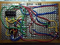
Left: The bottom of the board.
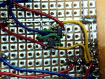
Right: A closer look at the regulators. I didn’t even bother adding filter capacitors on the outputs; maybe I will later.

Since I had a Sparkfun FT232RL  breakout board, I used that for comms (instead of having the FTDI onboard like the original).


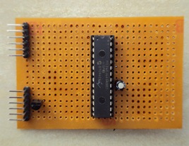
Pin headers, the LP2950, a PIC24FJ64GA002, and a capacitor are on the top.

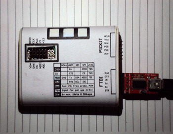
The top of the board. Visible are right angled pin headers (the top left one is for a PICKIT programmer, the bottom one is for the FTDI). Beside the

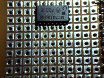
I also had a SOIC14 MC14066B from an old motherboard that I used in place of the CD4066.

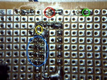
    Left: Prepping the 4066 for soldering onto veroboard. Each pad was cut in half. 
Right: some SMD components – 10kΩ voltage dividers for the ADC in blue; 470Ω for LED current limiting in green, a 0.22uF ceramic in the yellow circle, and the blue LEDs in red.

A few cosmetic changes, like blue status LEDs, and juggling the BP header pins about, were also necessary; but the general idea remains unchanged.


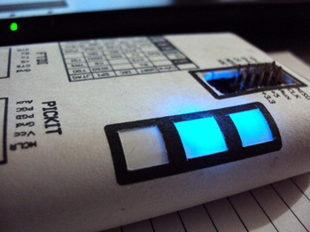
The ‘Power’ and ‘Mode’ LEDs lit up. I forgot to name the LEDs on the paper decal.

The case is an artificial sweetener box swiped from mom’s kitchen and repurposed with my Dremel. Slots were cut into either end to hold the veroboard in place. An opening was cut in at the top, allowing the header to poke out. Two smaller openings were made for headers to the FTDI and a PICkit2.

sweetner  case
Left:The original case, and Right: after being sanded and cleaned.

Once built, I programmed the PIC24FJ64GA002 with my trusty PICKit2. Firmware v5.10 was uploaded using ds30Loader. My BP passed the self tests without so much as a whimper.

To try out its features I decided to continue fooling around with the BU2090.

Driving the BU2090FS with a BP
Configuring the BP was simple enough. When I was greeted with HiZ> on the main prompt I changed mode to 2WIRE by pressing m and then 6. I pressed 4 to get the fastest available speed – 400kHz, and made the outputs ‘normal’ by entering 2.

BP setup
Configuring the Bus Pirate

It was now a simple task entering special characters (_ – / \) to toggle the DATA and CLK lines the way I wanted.

The ‘2090 shifts one bit of data at a time.
To shift in a ‘0’ the keystrokes used by the BP are: _/_\.
To shift in a ‘1’ they are: –/_\.

Once data is shifted in it needs to be latched to the outputs.
To shift in a ‘0’ and latch all the data (including the recently shifted bit):_/-\.
To shift and latch a ‘1’: –/-\.

So if I wanted to get the following binary output from the 12-bit output of the ‘2090: 1 1 0 1 0 0 0 0 0 1 1 1, I’d use the following syntax:

–/_\–/_\_/_\–/_\_/_\_/_\_/_\_/_\_/_\–/_\–/_\–/-\
     1      1       0       1       0      0       0      0       0      1       1      1L
  MSB                                                                                           LSB

I’ve depicted alternate bits in different colours for clarity. Data is left-shifted MSB-first. The last ‘1’ to be shifted in latches data to the outputs. A quick video of data being shifted in is on it way, but you’ll have to make do with a still for the time being.


Data shifted in

Of course, this may not be the most efficient way to control the ‘2090 with the BP; there may be shorter command sequences, and better modes. Please post in the comments if you know of a better way.

Saturday, June 25, 2011

Using the BU2090FS LED shift driver

I do a lot of scavenging for components. Whenever I get my hands on junk electronics I whip out my soldering iron, a desoldering pump, some pliers, and a pair of tweezers to see what I can extract from it. Scavenging is a long, tedious and sometimes painful process involving singed hair and burnt fingers, but every once in a while I come across a really nice component from an old TV or washing machine. I’ve learned a lot of desoldering (and some soldering) skills, and managed to save a few bucks by scavenging for components.

IIRC, I found the BU2090FS on a VCR board. I managed to desolder the SSOP16 chip by throwing the entire PCB into a toaster. I let the board cook for a few minutes and then started pulling off parts with my tweezers. The chip is quite solderable by hand, but I had no 0.8mm SSOP boards, so I superglued the chip onto veroboard and had a go at hand soldering the thing.

BU2090F-E2

Now you’re probably thinking that hand soldering a 16 pin SSOP is a daunting job, but its not really that hard. All you need is a fine point soldering tip and a steady hand. A little bit of magnification and good lighting helps as well. All in all it took me less than 15 minutes to make the DIY SSOP-to-dip ‘adaptor’.

DSC01430 DSC01425
Left: the ‘adaptor’
Right: the chip can be seen below the wires

The ‘2090 is a 12-bit latched shift register, and is primarily used to drive LEDs. It runs off 5v and can sink upto 25mA per channel. Coding for the chip wasn’t difficult at all. Serial data can simply be clocked in and you’re ready to go.

Below is a ‘scope capture of the data to make output Q8 and Q0 low. Data is fed in MSB-first. Keep in mind that the outputs are active low since this is a sinking driver.

scope

 Oscilloscope capture

Data and clock lines idle low. According to the datasheet data is sampled every rising clock. A shift occurs after every new bit of data is clocked in. Data is latched after all 12 bits are sampled by raising data high and then pulling clock low.

I used CCS-C on a PIC16F882 to test the chip. An excerpt of the driver is below:

#define clk pin_c5
#define data pin_c4

void writedata (int16 var)
{
    int8 loop;

    var<<=4;   

    for(loop=0;loop<11;loop++)
    {
        output_bit(data,var&0x8000);
        output_high(clk);
        output_low(data);
        output_low(clk);
        var<<=1;
    }
    output_bit(data,var&0x8000);
    output_high(clk);
    output_high(data);
    output_low(clk);
}


DSC01427  DSC01428
The BUF2090 mounted for prototyping

Saturday, June 18, 2011

Cheap Graphics – Nokia 3310 LCD

It’s been aeons since I blogged last. I’ve kinda gotten rusty so I thought I’d begin small by blogging about something that’s been a work-in-progress for a quite a while.

I’m always looking for inexpensive ways to add ‘bling’ to my projects. A graphic LCD is a lovely way to add that extra bit of fun (and functionality) to an application. Granted, a graphical display may be total overkill in some situations, and may not even be required in others. But when it is necessary, the Nokia 3310 display is a cheap and easy way to display 48*84 pixels of graphics.

I’m not going to go into the specifics of driving the 3310 LCD – I simply followed the resource found online. Scroll to the end of this post to see what’s helped me out. In this post I’m going to condense the four years of dilly-dallying and playing around that was a ‘necessary’ prerequisite in learning to interface the 3310.

I bought my LCD from Lajpat Rai market in Old Delhi for Rs.120 (less than $3) from a mobile repair shop. If I had haggled I may have got it for 80 bucks. It took me two whole years to actually get down to interfacing it – the main thing that made me repeatedly postpone working on the LCD was the difficulty in interfacing. The pic below shows what I achieved in January of 2010. I used LCDInfo and connected the 3310 LCD to the parallel port of my IBM. The results were far from pretty, but I liked what I saw.

Messy wiringMy first attempt: messy, to say the least.

Again, my reluctance to work on this seriously was due to the fiddly wires and temperamental connections. So I made the connections slightly more reliable by using the plastic chassis of the phone and soldering a ribbon cable to the connector (which, by the way, is not too difficult).

TP1         TP2

TP3
The LCD being tested. Read more about how I interfaced a touchpad here.

In May of 2010 I used a touch pad and interfaced the LCD to it with a PIC. Pretty fun stuff. Here’s the post and a video. The LCD, however, still had a mind of its own, and would abruptly stop working due to poor connections.

Finally, a year later (in June 2011) I got down to making something much more reliable; something that would allow me to easily prototype with the LCD. Here are the results.

Top   Bottom
The LCD board.
Left: Top. Right: Bottom showing header.

LCD connector   Comparision
The LCD spring connector. Hand soldered and compared to a pen.

Marked   Sub assy
Left:
the veroboard marked for cutting with a Dremel.
Right: parts of the assembly.

It took me only a couple of hours with a Dremel, some cyanoacrylate glue, veroboard and some headers to make this. Now I can simply stick the board into a solderless breadboard. A backlight is missing, and is the order of business tomorrow. :-)

Resources:

Visitors